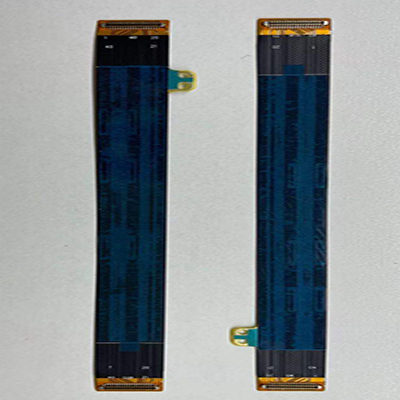
FPC wiring surface common defects and solutions
1. Bubbles are formed after side expansion of FPC row lines or single lines
Main reason: THE FPC line in two or more than two lines between the bubble, mainly because of the narrow line spacing, line is too high, so that the screen printing can not be printed on the substrate solder resist, resulting in air or moisture between the solder and the substrate. Gas thermal expansion during curing and exposure is mainly caused by overheight lines. When the blade is in contact with the line, the included Angle between the scraper and the wire increases, so that the solder resist can not be printed to the root of the line, so that there is gas between the root of the weld and the weld resist layer, and bubbles are generated after heating.

Solution: when screen printing, it is necessary to check whether screen material is completely printed on the substrate and the side wall of the line, and strictly control the current when electroplating.
2, FPC line hole, with resistance welding and graphic pinhole
The main reason is: FPC line in the screen printing process does not print paper in time, resulting in excessive accumulation of residual ink in the screen, the residual ink will be sent into the hole under the pressure of the scraper, and the number of screen is too small, will also cause welding resistance in the hole. There is dirt on the photographic baseplate, which causes the FPC line to fail to see light during the exposure process, resulting in pinholes in the pattern.
Solution: timely use of high mesh printing paper and screen, exposure often check the cleanliness of the photo.
3. The copper foil line under the resistance welding layer of FPC line appears black.
Main cause: THE FPC line is not dried after wiping, and the printed circuit board surface is splashed by liquid or manual forming before printing resistance welding.
Solution: FPC line screen printing on both sides of the printed board copper foil oxidation phenomenon.
Contact: Ms.Huang
Phone: 15023181892(微信同號)
Tel: 0755-23289186
Email: [email protected]
Add: xingye road,14th,bao'an shenzhen city CHINA